US9097698B2 - Nanogap device with capped nanowire structures - Google Patents
Nanogap device with capped nanowire structures Download PDFInfo
- Publication number
- US9097698B2 US9097698B2 US14/608,781 US201514608781A US9097698B2 US 9097698 B2 US9097698 B2 US 9097698B2 US 201514608781 A US201514608781 A US 201514608781A US 9097698 B2 US9097698 B2 US 9097698B2
- Authority
- US
- United States
- Prior art keywords
- nanowire
- capped
- retraction
- nanogap
- dielectric membrane
- Prior art date
- Legal status (The legal status is an assumption and is not a legal conclusion. Google has not performed a legal analysis and makes no representation as to the accuracy of the status listed.)
- Active
Links
- 239000002070 nanowire Substances 0.000 title claims abstract description 146
- 239000000463 material Substances 0.000 claims abstract description 80
- 239000012528 membrane Substances 0.000 claims abstract description 68
- 239000004065 semiconductor Substances 0.000 claims description 67
- 239000000758 substrate Substances 0.000 claims description 50
- 229910052751 metal Inorganic materials 0.000 claims description 37
- 239000002184 metal Substances 0.000 claims description 37
- KDLHZDBZIXYQEI-UHFFFAOYSA-N Palladium Chemical compound [Pd] KDLHZDBZIXYQEI-UHFFFAOYSA-N 0.000 claims description 21
- 229910052763 palladium Inorganic materials 0.000 claims description 11
- BASFCYQUMIYNBI-UHFFFAOYSA-N platinum Chemical compound [Pt] BASFCYQUMIYNBI-UHFFFAOYSA-N 0.000 claims description 8
- 229910052581 Si3N4 Inorganic materials 0.000 claims description 5
- HQVNEWCFYHHQES-UHFFFAOYSA-N silicon nitride Chemical compound N12[Si]34N5[Si]62N3[Si]51N64 HQVNEWCFYHHQES-UHFFFAOYSA-N 0.000 claims description 5
- 229910052697 platinum Inorganic materials 0.000 claims description 4
- NRTOMJZYCJJWKI-UHFFFAOYSA-N Titanium nitride Chemical compound [Ti]#N NRTOMJZYCJJWKI-UHFFFAOYSA-N 0.000 claims description 3
- TWNQGVIAIRXVLR-UHFFFAOYSA-N oxo(oxoalumanyloxy)alumane Chemical compound O=[Al]O[Al]=O TWNQGVIAIRXVLR-UHFFFAOYSA-N 0.000 claims description 3
- 229910052710 silicon Inorganic materials 0.000 claims description 3
- 239000010703 silicon Substances 0.000 claims description 2
- 230000005641 tunneling Effects 0.000 abstract description 10
- 238000001712 DNA sequencing Methods 0.000 abstract description 6
- 230000004888 barrier function Effects 0.000 abstract description 4
- 238000005259 measurement Methods 0.000 abstract description 4
- 230000007774 longterm Effects 0.000 abstract description 3
- 108020004414 DNA Proteins 0.000 description 23
- 102000053602 DNA Human genes 0.000 description 23
- 238000000034 method Methods 0.000 description 22
- 239000011241 protective layer Substances 0.000 description 18
- 239000010410 layer Substances 0.000 description 16
- 238000005520 cutting process Methods 0.000 description 15
- 230000008569 process Effects 0.000 description 12
- VYPSYNLAJGMNEJ-UHFFFAOYSA-N Silicium dioxide Chemical compound O=[Si]=O VYPSYNLAJGMNEJ-UHFFFAOYSA-N 0.000 description 10
- 238000005530 etching Methods 0.000 description 9
- 238000000059 patterning Methods 0.000 description 9
- 239000001307 helium Substances 0.000 description 8
- 229910052734 helium Inorganic materials 0.000 description 8
- WGTYBPLFGIVFAS-UHFFFAOYSA-M tetramethylammonium hydroxide Chemical compound [OH-].C[N+](C)(C)C WGTYBPLFGIVFAS-UHFFFAOYSA-M 0.000 description 8
- 238000005229 chemical vapour deposition Methods 0.000 description 7
- -1 helium ion Chemical class 0.000 description 6
- 150000004767 nitrides Chemical class 0.000 description 6
- 229920002120 photoresistant polymer Polymers 0.000 description 6
- 238000012163 sequencing technique Methods 0.000 description 6
- 238000005137 deposition process Methods 0.000 description 5
- 239000002019 doping agent Substances 0.000 description 5
- 238000012545 processing Methods 0.000 description 5
- 235000012239 silicon dioxide Nutrition 0.000 description 5
- 239000000377 silicon dioxide Substances 0.000 description 5
- 230000005540 biological transmission Effects 0.000 description 4
- 239000007853 buffer solution Substances 0.000 description 4
- 230000008859 change Effects 0.000 description 4
- 239000003989 dielectric material Substances 0.000 description 4
- PCHJSUWPFVWCPO-UHFFFAOYSA-N gold Chemical compound [Au] PCHJSUWPFVWCPO-UHFFFAOYSA-N 0.000 description 4
- 229910052737 gold Inorganic materials 0.000 description 4
- 239000010931 gold Substances 0.000 description 4
- 238000010884 ion-beam technique Methods 0.000 description 4
- 238000001459 lithography Methods 0.000 description 4
- 238000005240 physical vapour deposition Methods 0.000 description 4
- 238000000623 plasma-assisted chemical vapour deposition Methods 0.000 description 4
- 229920002477 rna polymer Polymers 0.000 description 4
- 238000000231 atomic layer deposition Methods 0.000 description 3
- 238000000151 deposition Methods 0.000 description 3
- 230000005684 electric field Effects 0.000 description 3
- RAXXELZNTBOGNW-UHFFFAOYSA-N imidazole Natural products C1=CNC=N1 RAXXELZNTBOGNW-UHFFFAOYSA-N 0.000 description 3
- 239000000126 substance Substances 0.000 description 3
- 238000012546 transfer Methods 0.000 description 3
- KXDAEFPNCMNJSK-UHFFFAOYSA-N Benzamide Chemical compound NC(=O)C1=CC=CC=C1 KXDAEFPNCMNJSK-UHFFFAOYSA-N 0.000 description 2
- FAPWRFPIFSIZLT-UHFFFAOYSA-M Sodium chloride Chemical compound [Na+].[Cl-] FAPWRFPIFSIZLT-UHFFFAOYSA-M 0.000 description 2
- 238000013459 approach Methods 0.000 description 2
- 238000000224 chemical solution deposition Methods 0.000 description 2
- 239000011248 coating agent Substances 0.000 description 2
- 238000000576 coating method Methods 0.000 description 2
- 150000001875 compounds Chemical class 0.000 description 2
- 230000008021 deposition Effects 0.000 description 2
- 238000009792 diffusion process Methods 0.000 description 2
- 238000000609 electron-beam lithography Methods 0.000 description 2
- 238000001704 evaporation Methods 0.000 description 2
- 230000008020 evaporation Effects 0.000 description 2
- 238000007672 fourth generation sequencing Methods 0.000 description 2
- SWQJXJOGLNCZEY-UHFFFAOYSA-N helium atom Chemical compound [He] SWQJXJOGLNCZEY-UHFFFAOYSA-N 0.000 description 2
- 238000004519 manufacturing process Methods 0.000 description 2
- 229910001092 metal group alloy Inorganic materials 0.000 description 2
- 150000002739 metals Chemical class 0.000 description 2
- 239000002773 nucleotide Substances 0.000 description 2
- 125000003729 nucleotide group Chemical group 0.000 description 2
- 230000003647 oxidation Effects 0.000 description 2
- 238000007254 oxidation reaction Methods 0.000 description 2
- 230000000737 periodic effect Effects 0.000 description 2
- 238000001020 plasma etching Methods 0.000 description 2
- 102000004169 proteins and genes Human genes 0.000 description 2
- 108090000623 proteins and genes Proteins 0.000 description 2
- 239000000243 solution Substances 0.000 description 2
- 238000004544 sputter deposition Methods 0.000 description 2
- 229910052723 transition metal Inorganic materials 0.000 description 2
- 150000003624 transition metals Chemical class 0.000 description 2
- 229910001218 Gallium arsenide Inorganic materials 0.000 description 1
- 229910000673 Indium arsenide Inorganic materials 0.000 description 1
- 206010028980 Neoplasm Diseases 0.000 description 1
- 239000013614 RNA sample Substances 0.000 description 1
- 229910003811 SiGeC Inorganic materials 0.000 description 1
- 229910000577 Silicon-germanium Inorganic materials 0.000 description 1
- 229910000681 Silicon-tin Inorganic materials 0.000 description 1
- 229910021607 Silver chloride Inorganic materials 0.000 description 1
- 108020004682 Single-Stranded DNA Proteins 0.000 description 1
- ATJFFYVFTNAWJD-UHFFFAOYSA-N Tin Chemical compound [Sn] ATJFFYVFTNAWJD-UHFFFAOYSA-N 0.000 description 1
- 238000004458 analytical method Methods 0.000 description 1
- 238000004380 ashing Methods 0.000 description 1
- 201000011510 cancer Diseases 0.000 description 1
- 238000003486 chemical etching Methods 0.000 description 1
- 239000013078 crystal Substances 0.000 description 1
- 229910021419 crystalline silicon Inorganic materials 0.000 description 1
- 230000004069 differentiation Effects 0.000 description 1
- 201000010099 disease Diseases 0.000 description 1
- 208000037265 diseases, disorders, signs and symptoms Diseases 0.000 description 1
- 230000000694 effects Effects 0.000 description 1
- 239000012777 electrically insulating material Substances 0.000 description 1
- 239000007772 electrode material Substances 0.000 description 1
- 239000003792 electrolyte Substances 0.000 description 1
- 238000005516 engineering process Methods 0.000 description 1
- 239000012530 fluid Substances 0.000 description 1
- 239000007789 gas Substances 0.000 description 1
- 229910052732 germanium Inorganic materials 0.000 description 1
- 238000000227 grinding Methods 0.000 description 1
- 239000011799 hole material Substances 0.000 description 1
- RPQDHPTXJYYUPQ-UHFFFAOYSA-N indium arsenide Chemical compound [In]#[As] RPQDHPTXJYYUPQ-UHFFFAOYSA-N 0.000 description 1
- 150000002500 ions Chemical class 0.000 description 1
- 238000000608 laser ablation Methods 0.000 description 1
- 229910003465 moissanite Inorganic materials 0.000 description 1
- 239000002090 nanochannel Substances 0.000 description 1
- 230000003287 optical effect Effects 0.000 description 1
- 150000002940 palladium Chemical class 0.000 description 1
- 238000007747 plating Methods 0.000 description 1
- 239000011148 porous material Substances 0.000 description 1
- 238000002360 preparation method Methods 0.000 description 1
- 238000009877 rendering Methods 0.000 description 1
- 230000000717 retained effect Effects 0.000 description 1
- 239000012266 salt solution Substances 0.000 description 1
- 239000000523 sample Substances 0.000 description 1
- 229910010271 silicon carbide Inorganic materials 0.000 description 1
- 229910052709 silver Inorganic materials 0.000 description 1
- 239000004332 silver Substances 0.000 description 1
- HKZLPVFGJNLROG-UHFFFAOYSA-M silver monochloride Chemical compound [Cl-].[Ag+] HKZLPVFGJNLROG-UHFFFAOYSA-M 0.000 description 1
- 239000011780 sodium chloride Substances 0.000 description 1
- 239000007787 solid Substances 0.000 description 1
Images


Classifications
-
- G—PHYSICS
- G01—MEASURING; TESTING
- G01N—INVESTIGATING OR ANALYSING MATERIALS BY DETERMINING THEIR CHEMICAL OR PHYSICAL PROPERTIES
- G01N33/00—Investigating or analysing materials by specific methods not covered by groups G01N1/00 - G01N31/00
- G01N33/48—Biological material, e.g. blood, urine; Haemocytometers
- G01N33/483—Physical analysis of biological material
- G01N33/487—Physical analysis of biological material of liquid biological material
- G01N33/48707—Physical analysis of biological material of liquid biological material by electrical means
- G01N33/48721—Investigating individual macromolecules, e.g. by translocation through nanopores
-
- B—PERFORMING OPERATIONS; TRANSPORTING
- B01—PHYSICAL OR CHEMICAL PROCESSES OR APPARATUS IN GENERAL
- B01L—CHEMICAL OR PHYSICAL LABORATORY APPARATUS FOR GENERAL USE
- B01L3/00—Containers or dishes for laboratory use, e.g. laboratory glassware; Droppers
- B01L3/50—Containers for the purpose of retaining a material to be analysed, e.g. test tubes
- B01L3/502—Containers for the purpose of retaining a material to be analysed, e.g. test tubes with fluid transport, e.g. in multi-compartment structures
- B01L3/5027—Containers for the purpose of retaining a material to be analysed, e.g. test tubes with fluid transport, e.g. in multi-compartment structures by integrated microfluidic structures, i.e. dimensions of channels and chambers are such that surface tension forces are important, e.g. lab-on-a-chip
- B01L3/502707—Containers for the purpose of retaining a material to be analysed, e.g. test tubes with fluid transport, e.g. in multi-compartment structures by integrated microfluidic structures, i.e. dimensions of channels and chambers are such that surface tension forces are important, e.g. lab-on-a-chip characterised by the manufacture of the container or its components
-
- B—PERFORMING OPERATIONS; TRANSPORTING
- B81—MICROSTRUCTURAL TECHNOLOGY
- B81C—PROCESSES OR APPARATUS SPECIALLY ADAPTED FOR THE MANUFACTURE OR TREATMENT OF MICROSTRUCTURAL DEVICES OR SYSTEMS
- B81C1/00—Manufacture or treatment of devices or systems in or on a substrate
- B81C1/00015—Manufacture or treatment of devices or systems in or on a substrate for manufacturing microsystems
- B81C1/00206—Processes for functionalising a surface, e.g. provide the surface with specific mechanical, chemical or biological properties
-
- H—ELECTRICITY
- H01—ELECTRIC ELEMENTS
- H01L—SEMICONDUCTOR DEVICES NOT COVERED BY CLASS H10
- H01L29/00—Semiconductor devices adapted for rectifying, amplifying, oscillating or switching, or capacitors or resistors with at least one potential-jump barrier or surface barrier, e.g. PN junction depletion layer or carrier concentration layer; Details of semiconductor bodies or of electrodes thereof ; Multistep manufacturing processes therefor
- H01L29/02—Semiconductor bodies ; Multistep manufacturing processes therefor
- H01L29/06—Semiconductor bodies ; Multistep manufacturing processes therefor characterised by their shape; characterised by the shapes, relative sizes, or dispositions of the semiconductor regions ; characterised by the concentration or distribution of impurities within semiconductor regions
- H01L29/0657—Semiconductor bodies ; Multistep manufacturing processes therefor characterised by their shape; characterised by the shapes, relative sizes, or dispositions of the semiconductor regions ; characterised by the concentration or distribution of impurities within semiconductor regions characterised by the shape of the body
- H01L29/0665—Semiconductor bodies ; Multistep manufacturing processes therefor characterised by their shape; characterised by the shapes, relative sizes, or dispositions of the semiconductor regions ; characterised by the concentration or distribution of impurities within semiconductor regions characterised by the shape of the body the shape of the body defining a nanostructure
- H01L29/0669—Nanowires or nanotubes
-
- H—ELECTRICITY
- H01—ELECTRIC ELEMENTS
- H01L—SEMICONDUCTOR DEVICES NOT COVERED BY CLASS H10
- H01L29/00—Semiconductor devices adapted for rectifying, amplifying, oscillating or switching, or capacitors or resistors with at least one potential-jump barrier or surface barrier, e.g. PN junction depletion layer or carrier concentration layer; Details of semiconductor bodies or of electrodes thereof ; Multistep manufacturing processes therefor
- H01L29/40—Electrodes ; Multistep manufacturing processes therefor
- H01L29/41—Electrodes ; Multistep manufacturing processes therefor characterised by their shape, relative sizes or dispositions
- H01L29/413—Nanosized electrodes, e.g. nanowire electrodes comprising one or a plurality of nanowires
-
- B—PERFORMING OPERATIONS; TRANSPORTING
- B01—PHYSICAL OR CHEMICAL PROCESSES OR APPARATUS IN GENERAL
- B01L—CHEMICAL OR PHYSICAL LABORATORY APPARATUS FOR GENERAL USE
- B01L2300/00—Additional constructional details
- B01L2300/06—Auxiliary integrated devices, integrated components
- B01L2300/0627—Sensor or part of a sensor is integrated
- B01L2300/0645—Electrodes
-
- B—PERFORMING OPERATIONS; TRANSPORTING
- B01—PHYSICAL OR CHEMICAL PROCESSES OR APPARATUS IN GENERAL
- B01L—CHEMICAL OR PHYSICAL LABORATORY APPARATUS FOR GENERAL USE
- B01L2300/00—Additional constructional details
- B01L2300/08—Geometry, shape and general structure
- B01L2300/0896—Nanoscaled
-
- B—PERFORMING OPERATIONS; TRANSPORTING
- B81—MICROSTRUCTURAL TECHNOLOGY
- B81B—MICROSTRUCTURAL DEVICES OR SYSTEMS, e.g. MICROMECHANICAL DEVICES
- B81B2201/00—Specific applications of microelectromechanical systems
- B81B2201/02—Sensors
- B81B2201/0214—Biosensors; Chemical sensors
-
- B—PERFORMING OPERATIONS; TRANSPORTING
- B81—MICROSTRUCTURAL TECHNOLOGY
- B81B—MICROSTRUCTURAL DEVICES OR SYSTEMS, e.g. MICROMECHANICAL DEVICES
- B81B2203/00—Basic microelectromechanical structures
- B81B2203/03—Static structures
- B81B2203/0353—Holes
Definitions
- the present application relates to a nanodevice, and more particularly, to a sub-3 nm nanogap device containing capped nanowire structures located on a surface of a dielectric membrane.
- Nanopore sequencing is a method for determining the order in which nucleotides occur on a strand of deoxyribonucleic acid (DNA).
- a nanopore also referred to as pore, nanochannel, hole, etc.
- a nanopore sequencing is about what occurs when the nanopore is submerged in a conducting fluid and an electric potential (voltage) is applied across the nanopore. Under these conditions, a slight electric current due to conduction of ions through the nanopore can be measured, and the amount of current is very sensitive to the size and shape of the nanopore.
- the DNA can be driven through the nanopore by using various methods, so that the DNA might eventually pass through the nanopore.
- the scale of the nanopore can have the effect that the DNA may be forced through the hole as a long string, one base at a time, like a thread through the eye of a needle.
- An anti-retraction capping material is formed on a surface of a nanowire that is located upon a dielectric membrane. A gap is then formed into the anti-retraction capping material and nanowire forming first and second capped nanowire structures of a nanodevice.
- the nanodevice can be used for recognition tunneling measurements including, for example DNA sequencing.
- the anti-retraction capping material serves as a mobility barrier to pin, i.e., confine, a nanowire portion of each of the first and second capped nanowire structures in place, allowing long-term structural stability. In some embodiments, interelectrode leakage through solution during recognition tunneling measurements can be minimized.
- a method of forming a nanogap device includes providing a dielectric membrane on a front-side surface of a semiconductor substrate. A nanowire is then formed on a surface of the dielectric membrane. An anti-retraction capping material is deposited on an upper surface of the nanowire. Next, the anti-retraction capping material and the nanowire are cut to provide a first capped nanowire structure and a second capped nanowire structure. The first capped nanowire structure and the second capped nanowire structure are separated by a nanogap of less than 3 nanometers.
- a nanogap device in another aspect of the present application, includes a dielectric membrane located on a front-side surface of a semiconductor substrate.
- a first capped nanowire structure is located on a first portion of the dielectric membrane, and a second capped nanowire structure is located on a second portion of the dielectric membrane.
- the first capped nanowire structure and the second capped nanowire structure are separated by a nanogap of less than 3 nanometers.
- FIG. 1 is a cross sectional view of a first exemplary structure including, from bottom to top, a semiconductor substrate and a dielectric membrane in accordance with an embodiment of the present application.
- FIG. 2 is a cross sectional view of the first exemplary structure of FIG. 1 after forming a protective layer on the dielectric membrane.
- FIG. 3 is a cross sectional view of the first exemplary structure of FIG. 2 after rotating the structure 180° and forming a hard mask on a surface of the semiconductor substrate opposite the surface containing the dielectric membrane.
- FIG. 4 is a cross sectional view of the first exemplary structure of FIG. 3 after patterning the hard mask.
- FIG. 5 is a cross sectional view of the first exemplary structure of FIG. 4 after providing an opening within the semiconductor substrate using remaining portions of the hard mask as an etch mask.
- FIG. 6 is a cross sectional view of the first exemplary structure of FIG. 5 after removing the remaining portions of the hard mask, rotating the structure 180° and removing the protective layer.
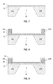
- FIG. 7 is a cross sectional view of the first exemplary structure of FIG. 6 after forming a nanowire.
- FIG. 8 is a cross sectional view of the first exemplary structure of FIG. 7 after forming metal pads on portions of the nanowire.
- FIG. 9 is a cross sectional view of the first exemplary structure of FIG. 8 after coating the nanowire and metal pads with an anti-retraction capping material.
- FIG. 10 is a cross sectional view of the first exemplary structure of FIG. 9 after cutting the anti-retraction capping material and the nanowire to provide a first capped nanowire structure and a second capped nanowire structure, wherein the first capped nanowire structure and the second capped nanowire structure are separated by a nanogap of less than 3 nanometers.
- FIG. 11 is a cross sectional view of the first exemplary structure of FIG. 10 after forming a first linker molecule on an exposed edge of a first nanowire portion of the first capped nanowire structure and a second linker molecule on an exposed edge of a second nanowire portion of the second capped nanowire structure.
- FIG. 12 illustrates a sequencing system utilizing the nanodevice according to an embodiment of the present application.
- FIG. 13 is a plot of nanogap size (nm) vs. time in air (hours) for a nanodevice including a capped nanowire structure (in accordance with the present application) and for a nanodevice including a non-capped nanowire structure (not in accordance with the present application).
- Single-based tunneling recognition is one approach that can be used to enable high-through-put, low-cost DNA sequencing because it reduces the amount of preparation that a target DNA requires to ready it from sequencing, i.e., copying is not necessary.
- STM scanning tunneling microscope
- the failure to reproduce this capability on a technologically relevant platform has stemmed, in large part, from fabrication challenges that appear in structures with dimensions in the few nanometer range.
- DNA sequencing by tunneling recognition on a manufacturable platform requires that the signature tunneling current from each individual base be read by a tunneling gap electrode which must be less than 3 nm wide and able to maintain a fixed gap width.
- palladium and gold are considered to be ideal candidates for DNA sensing because such conductive metals are excellent linkers for chemicals that are used to functionalize the electrodes, which are needed to ready the electrodes for DNA base differentiation; however, nanoscale surface mobility represents a major concern for these materials.
- the extraordinary high surface mobility of gold make it less attractive than palladium for maintaining a fixed-gap width.
- palladium fairs a bit better in this respect, it has been recently discovered that a 3 nm gap cut in palladium nanowires results in retraction or widening of the gap by 0.7 to 2.5 nm after 1 day in air, rendering the gap size too large for the purposes of DNA sequencing.
- This stability issue is a major problem from a manufacturing perspective as well, wherein commercialization may not be possible due to yield and instability issues.
- the present application provides a method and structure that address the above stability issue.
- FIG. 1 there is illustrated a first exemplary structure including, from bottom to top, a semiconductor substrate 10 and a dielectric membrane 12 in accordance with an embodiment of the present application.
- the dielectric membrane 12 is formed as a contiguous dielectric layer on a front-side surface of the semiconductor substrate 10 .
- the term “front-side surface of the semiconductor substrate” denotes a surface of the semiconductor substrate 10 in which there is present an interface with the dielectric membrane 12 .
- the term “back-side surface of the semiconductor substrate” denotes a surface of the semiconductor substrate 10 that opposes the surface containing the interface with the dielectric membrane 12 .
- the semiconductor substrate 10 that can be used in the present application can be a bulk semiconductor substrate.
- the term “bulk” denotes that the entirety of the semiconductor substrate 10 is comprised of a semiconductor material.
- semiconductor materials that can be employed as the semiconductor substrate include, but not limited to, Si, Ge, SiGe, SiC, SiGeC, and III/V compound semiconductors such as, for example, InAs, GaAs, and InP. Multilayers of these semiconductor materials can also be used as the semiconductor material of the bulk semiconductor.
- the semiconductor substrate 10 can be comprised of a single crystalline semiconductor material, such as, for example, single crystalline silicon.
- the semiconductor substrate 10 may comprise a polycrystalline or amorphous semiconductor material.
- semiconductor substrate 10 may comprise a multilayered stack of semiconductor materials that are in epitaxial alignment with each other.
- the semiconductor substrate 10 may have any crystal orientation including, for example, ⁇ 100 ⁇ , ⁇ 110 ⁇ , or ⁇ 111 ⁇ . Other crystallographic orientations besides those specifically mentioned can also be used in the present application for the semiconductor substrate 10 .
- the semiconductor substrate 10 that is employed in the present application may be an intrinsic semiconductor material.
- intrinsic it is meant that the semiconductor substrate 10 has a dopant concentration of less than 1 ⁇ 10 15 atoms/cm 3 .
- the semiconductor substrate 10 may contain a p-type dopant or an n-type dopant.
- the dopant may be uniformly distributed throughout the entirety of the semiconductor substrate 10 or the dopant may be present as a gradient.
- the dielectric membrane 12 that is present on the front-side surface of the semiconductor substrate 10 may be comprised of a semiconductor oxide, a semiconductor nitride and/or a semiconductor oxynitride.
- the dielectric membrane 12 may be comprised of silicon dioxide.
- the dielectric membrane 12 can be comprised of silicon nitride.
- the dielectric membrane 12 can be formed on the front-side surface of the semiconductor substrate 10 utilizing a deposition such as, for example, chemical vapor deposition, plasma enhanced chemical vapor deposition, or evaporation.
- the dielectric membrane 12 can be formed by a thermal growth process such as, for example, thermal oxidation and/or thermal nitridation.
- the dielectric membrane 12 that is formed at this point of the present application is a contiguous layer.
- the dielectric membrane 12 that is formed may have a thickness from 5 nm to 200 nm. Other thicknesses that are lesser than or greater than the aforementioned thickness range can also be used for the dielectric membrane 12 of the present application.
- the protective layer 14 that can be used in the present application comprises a different material than that of the dielectric membrane 12 .
- the protective layer 14 that is employed in the present application includes any material such as, for example, a dielectric material and/or a diffusion barrier material, which can prevent any damage to the dielectric membrane 12 during subsequently performed processing steps that are performed on the back-side surface of the semiconductor substrate 10 .
- the protective layer 14 should also have high etch selectivity compared with the dielectric membrane 12 so that it can be removed when back-side processing is complete without any thinning of the dielectric membrane 12 .
- the protective layer 14 may comprise an oxide, such as, for example, silicon dioxide.
- the protective layer 14 may include a multilayered stack of, from bottom to top, an oxide and a metal nitride.
- the protective layer 14 may include a multilayered stack of, from bottom to top, silicon dioxide and TiN.
- the protective layer 14 can be formed on an exposed upper surface of the dielectric membrane 12 utilizing well known deposition processes. For example, a chemical vapor deposition process utilizing tetraethylorthosilate (TEOS) or other silicon dioxide forming gases can be used. When a metal nitride is used as a portion of the protective layer 14 , the metal nitride can be formed utilizing a deposition process such as, for example, chemical vapor deposition, plasma enhanced chemical vapor deposition, physical vapor deposition or chemical solution deposition.
- TEOS tetraethylorthosilate
- the protective layer 14 that is formed may have a thickness from 500 nm to 700 nm. Other thicknesses that are lesser than or greater than the aforementioned thickness range can also be used for the protective layer 14 of the present application.
- FIG. 3 there is illustrated the first exemplary structure of FIG. 2 after rotating the structure 180° and forming a hard mask 16 on a surface (i.e., back-side surface) of the semiconductor substrate 10 opposite the surface containing the dielectric membrane 12 .
- the hard mask 16 is a contiguous layer that covers an entirety of the back-side surface of the semiconductor substrate 10 that is opposite the surface of the semiconductor substrate 10 including dielectric membrane 12 .
- the rotating of the structure shown in FIG. 2 by 180° may be performed by hand or by any mechanical means including, for example, a robot arm.
- the hard mask 16 may include a dielectric oxide, a dielectric nitride, a dielectric oxynitride or any multilayered combination thereof.
- the hard mask 16 may comprise a different dielectric material than the dielectric membrane 12 .
- the hard mask 16 may comprise a same dielectric material as the dielectric membrane 12 .
- the hard mask 16 is a dielectric oxide such as silicon dioxide, while in another embodiment the hard mask 16 is a dielectric nitride such as silicon nitride.
- the hard mask 16 can be formed utilizing a deposition process including, for example, chemical vapor deposition (CVD), plasma enhanced chemical vapor deposition (PECVD), chemical solution deposition, evaporation, or physical vapor deposition (PVD).
- CVD chemical vapor deposition
- PECVD plasma enhanced chemical vapor deposition
- PVD physical vapor deposition
- the hard mask 16 may be formed by one of thermal oxidation, and thermal nitridation.
- the thickness of the hard mask 16 employed in the present application may vary depending on the material of the hard mask 16 itself as well as the technique used in forming the same. Typically, and in one embodiment, the hard mask 16 has a thickness from 100 nm to 300 nm. Other thicknesses that are greater than or lesser than the aforementioned thickness range can also be used for the thickness of the hard mask 16 .
- FIG. 4 there is illustrated the first exemplary structure of FIG. 3 after patterning the hard mask 16 .
- the remaining portions of the hard mask 16 that are formed after patterning may be referred to herein as a first hard mask portion 16 L and a second hard mask portion 16 R.
- the first hard mask portion 16 L and the second hard mask portion 16 R that are provided can be used in a subsequent processing step as an etch mask.
- Patterning of the hard mask 16 can be performed by lithography and etching.
- Lithography can include forming a photoresist (not shown) on the topmost surface of the hard mask 16 , exposing the photoresist to a desired pattern, and then developing the exposed photoresist with a conventional resist developer to provide a patterned photoresist atop the hard mask 16 .
- An etch is then employed which transfers the pattern from the patterned photoresist into the hard mask 16 .
- the etch used for pattern transfer may include a dry etch process such as, for example, reactive ion etching, plasma etching, ion beam etching or laser ablation.
- the etch used for pattern transfer may include chemical etching process.
- TMAH tetramethylammonium hydroxide
- the patterned photoresist can be removed utilizing a resist stripping process such as, for example, ashing.
- FIG. 5 there is illustrated the first exemplary structure of FIG. 4 after providing an opening 18 within the semiconductor substrate 10 using the remaining portions of the hard mask 16 L, 16 R as an etch mask.
- the opening 18 is formed inward from the back-side surface of semiconductor substrate 10 to the front-side surface of the semiconductor substrate 10 .
- the remaining portions of the semiconductor substrate 10 may be referred to herein as a first semiconductor material portion 10 L and a second semiconductor material portion 10 R.
- the opening 18 that is provided exposes a surface of the dielectric membrane 12 that is opposite the surface of the dielectric membrane 12 that includes the protective layer 14 .
- the opening 18 that is formed into the semiconductor substrate 10 may have sidewalls that are perpendicularly oriented to the bottom surface of the dielectric membrane 12 .
- the opening 18 that is formed into the semiconductor substrate 10 has tapered sidewalls.
- the tapering of the sidewalls of the opening 18 may expand outwards from the bottom surface of the dielectric membrane 12 to the back-side surface of the semiconductor substrate 10 such that a width of the opening 18 that is nearest to the bottommost surface of the dielectric membrane 12 is less than a width of the opening 18 that is nearest to the back-side surface of the semiconductor substrate 10 .
- the tapering of the sidewalls of the opening may contract outwards from the bottom surface of the dielectric membrane 12 to the back-side surface of the semiconductor substrate 10 such that a width of the opening 18 the is nearest to the bottommost surface of the dielectric membrane 12 is greater than a width of the opening 18 that is nearest to the back-side surface of the semiconductor substrate 10 . Notwithstanding the type of opening 18 formed, the opening 18 has a width that is greater than a width of a nanogap to be subsequently formed in the dielectric membrane 12 .
- the opening 18 that is formed into the semiconductor substrate 10 can be provided utilizing an etching process that is selective for removing semiconductor material as compared to remaining hard mask portions 16 L, 16 R and dielectric membrane 12 .
- the etch process may be an isotropic etch or an anisotropic etch.
- a crystallographic etch can be used in providing the opening 18 .
- crystallographic etch it is meant an etching process, typically a wet etch, in which etching occurs preferentially along selected crystallographic planes in a crystalline solid.
- the opening 18 can be formed utilizing tetramethylammonium hydroxide (TMAH).
- FIG. 6 there is illustrated the first exemplary structure of FIG. 5 after removing the remaining portions of the hard mask 16 L, 16 R, rotating the structure 180° and removing the protective layer 14 .
- the removal of the remaining portions of the hard mask 16 L, 16 R can be omitted and the remaining portions of the hard mask 16 L, 16 R can be left within the final nanodevice of the present application.
- the removal of the protective layer 14 from the structure exposes the upper surface of the dielectric membrane 12 .
- an etching process can be used to remove the remaining portions of the hard mask 16 L, 16 R from the structure.
- the rotating of the structure can be performed by hand or any mechanical means including, for example, a robot arm.
- the protective layer 14 can be removed by a planarization process such as, for example, chemical mechanical planarization and/or grinding. Alternatively, an etching process can be used to remove the protective layer 14 .
- FIG. 7 there is illustrated the first exemplary structure of FIG. 6 after forming a nanowire 20 on the exposed surface of the dielectric membrane 12 . It is noted that the nanowire 20 does not necessary span the entire length of the underlying dielectric membrane 12 . It is also noted that although a single nanowire 20 is described and illustrated, a plurality of nanowires 20 can be formed.
- the nanowire 20 may include at least one transition metal from Group VIB, VIII and IB of the Periodic Table of Elements. In one embodiment, the nanowire 20 is selected from the group consisting of palladium, platinum and/or gold.
- the nanowire 20 may include a single layered structure or it may include a multilayered structure including at least two different metals stack one on top of the other.
- the nanowire 20 can be formed be first forming a layer of nanowire material (not specifically shown) on an exposed surface of the dielectric membrane 12 utilizing a deposition process including, for example, chemical vapor deposition, plasma chemical vapor deposition, atomic layer deposition, physical vapor deposition, sputtering, or plating. After deposition the layer of nanowire material, the nanowire 20 can be formed by patterning the layer of nanowire material. In one embodiment of the present application, the patterning of the layer of nanowire material may include e-beam lithography and a lift-off technique. In another embodiment of the present application, the patterning of the layer of nanowire material may include lithography and etching.
- the nanowire 20 that is formed may have a height from 2 nm to 20 nm. Other heights that are lesser than or greater than the aforementioned range can also be used for the nanowire 20 of the present application.
- the nanowire 20 can have a length from 20 nm to 1000 nm.
- the width of nanowire 20 as measured from one sidewall surface of the nanowire 20 to an opposing sidewall surface of the nanowire 20 , can be from 2 nm to 50 nm.
- the metal pads 22 L, 22 R can be comprised of a same metal or metal alloy as the nanowire 20 .
- the metal pads 22 L, 22 R can be comprised of a different metal or metal alloy as nanowire 20 .
- the metal pads 22 L, 22 R can include at least one transition metal from Group VIB, VIII and IB of the Periodic Table of Elements.
- each metal pad 22 L, 22 R is selected from the group consisting of palladium, platinum and/or gold.
- the metal pads 22 L, 22 R that are formed have a thickness that is generally greater than the thickness of the nanowire 20 .
- the metal pads 22 L, 22 R can be formed utilizing the same techniques as mentioned above in forming the nanowire 20 . That is, the metal pads 22 L, 22 R can be formed by depositing a blanket layer of a metal pad material. The blanket layer of metal pad material is then patterned.
- the patterning of the blanket layer of metal pad material may include e-beam lithography and a lift-off technique.
- the patterning of the blanket layer of metal pad material may include lithography and etching.
- the anti-retraction capping material 24 is a contiguous layer that is formed on exposed surfaces (sidewalls and upper surface) of the nanowire 20 and exposed surfaces (sidewalls and upper surface) of each metal pad 22 L, 22 R.
- the anti-retraction capping material 24 is used in the present application to prevent the retraction of subsequently formed nanowire portions of the nanodevice of the present application during their use.
- the anti-retraction capping material 24 can also act as a mobility barrier to pin the nanowire portions (to be subsequently formed) in place, allowing long-term stability.
- the anti-retraction capping material 24 that is used in the present application has an adequate compressive stress and shares some covalent bonds with the nanowire 20 beneath it.
- equate compressive stress it is meant that a sufficient compressive stress is present to counteract the natural tendency of the nanowire material retract after a gap 26 has been formed.
- Covalent bonds between the nanowire 20 and anti-retraction capping material 24 are necessary for the capping material 24 to hold the cut nanowires 20 L, 20 R, to be subsequently formed in place.
- the anti-retraction capping material 24 may be a dielectric material. In other embodiments, the anti-retraction capping material 24 may be composed of a non-electrically insulating material.
- aluminum oxide can be used as the anti-retraction capping material 24 .
- titanium nitride can be used as the anti-retraction capping material 24 .
- silicon nitride can be used as the anti-retraction capping material 24 .
- Other materials which can prevent diffusion of conductive atoms from the nanowire 20 can be used as the anti-retraction capping material.
- the anti-retraction capping material 24 may be a single layered structure, or it can be a multilayered structure including at least two different anti-retraction capping materials stacked one atop of the other.
- anti-retraction capping material 24 may include a stack of, from bottom to top, a layer of silicon nitride and a layer of titanium nitride.
- the anti-retraction capping material 24 comprises a different material than that of the hard mask portions 16 L, 16 R.
- the anti-retraction capping material 24 can be formed by a deposition process such as, for example, sputtering or atomic layer deposition.
- the anti-retraction capping material 24 that is formed may have a thickness from 3 nm to 15 nm. Other thicknesses that are lesser than or greater than the aforementioned thickness range can also be used for the anti-retraction capping material 24 of the present application.
- FIG. 10 there is illustrated the first exemplary structure of FIG. 9 after cutting the anti-retraction capping material 24 and the nanowire 20 to provide a first capped nanowire structure and a second capped nanowire structure, wherein the first capped nanowire structure and the second capped nanowire structure are separated by a nanogap 26 of less than 3 nanometers.
- the nanogap 26 between the first capped nanowire structure and the second capped nanowire structure is from 0.2 nm to 2 nm.
- the nanogap 26 of the present application is formed through both the anti-retraction capping material 24 and the nanowire 20 .
- the first capped nanowire structure includes a first nanowire portion 20 L and a first anti-retraction capping material portion 24 L
- the second capped nanowire structure includes a second nanowire portion 20 R and a second anti-retraction capping material portion 24 R.
- the first and second nanowire portions 20 L, 20 R are used as the electrodes of the nanodevice of the present application.
- the first capped nanowire structure ( 20 L, 24 L) and the second capped nanowire structure ( 20 R, 24 R) can be formed by cutting the anti-retraction capping material 24 and the nanowire 20 .
- the cutting of the anti-retraction capping material 24 and the nanowire 20 may include a helium ion beam cutting process in which a helium ion microscope can be used.
- helium ions are irradiated from the helium ion microscope and are used in the present application in forming the nanogap 26 .
- Any conventional helium ion microscope including, for example, ORIONTM Helium Ion Microscope from Carl Zeiss SMT or the Multiple Ion Beam Microscopes from Carl Zeiss SMT can be used in the present application.
- a voltage from 10 kilovolts to 30 kilovolts, a beam current of from 25 pA (picoamperes) to 1500 pA, a beam spot size of from 3.4 ⁇ to 5 ⁇ , a step size of from 5 ⁇ to 50 ⁇ , a working distance of from 5 millimeters to 10 millimeters, an aperture opening from 7.5 micrometers to 30 micrometers, and a exposure time from 0.5 ⁇ s/pixel to 2.0 ⁇ s/pixel can be used in the present application in providing the nanogap 26 through both the anti-retraction capping material 24 and the nanowire 20 .
- the cutting of the anti-retraction capping material 24 and the nanowire 20 may include the use of a focused transmission electron microscope (TEM) beam cutting process.
- TEM focused transmission electron microscope
- any conventional focused transmission electron microscope (TEM) beam cutting apparatus can be used.
- the conditions that can be used when a focused transmission electron microscope (TEM) beam cutting apparatus is employed in forming the nanogap 26 vary and can be optimized to provide a nanogap having a dimension of 3 nm or less.
- the cutting of the anti-retraction capping material 24 and the nanowire 20 may include the use of a combination of a helium ion beam cutting and focused transmission electron microscope (TEM) beam cutting.
- TEM focused transmission electron microscope
- FIG. 11 there is illustrated the first exemplary structure of FIG. 10 after forming a first linker molecule L 1 on an exposed edge of the first nanowire portion 20 L of the first capped nanowire structure and a second linker molecule L 2 on an exposed edge of the second nanowire portion 20 R of the second capped nanowire structure.
- linker molecule denotes a thiolated chemical compound.
- the first and second linker molecules L 1 , L 2 that can be employed in the present application include, for example, imidazole or benzamide.
- the first and second linker molecules L 1 , L 2 can be provided to the exposed edge of the first nanowire portion 20 L of the first capped nanowire structure and the exposed edge of the second nanowire portion 20 R of the second capped nanowire structure by covalent binding.
- FIGS. 10 and 11 illustrate a nanogap device in accordance with the present application.
- the nanogap device includes a dielectric membrane 12 located on a front-side surface of a semiconductor substrate 10 L, 10 R.
- a first capped nanowire structure ( 20 L and 24 L) is located on a first portion of the dielectric membrane 12
- a second capped nanowire structure 20 R and 24 R
- the first capped nanowire structure ( 20 L and 24 L) and the second capped nanowire structure 20 R and 24 R) are separated by a nanogap 26 of less than 3 nanometers.
- the nanodevice includes a dielectric membrane 12 located on a front-side surface of a semiconductor substrate 10 L, 10 R.
- a first capped nanowire structure ( 20 L and 24 L) is located on a first portion of the dielectric membrane 12
- a second capped nanowire structure is located on a second portion of the dielectric membrane.
- the first capped nanowire structure ( 20 L and 24 L) and the second capped nanowire structure 20 R and 24 R) are separated by a nanogap 26 of less than 3 nanometers.
- a backside cavity provided by opening 18 between semiconductor material portions 10 L, 10 R forms a suspended membrane making up the nanogap.
- a top reservoir 54 is attached and sealed to the top of each anti-retraction capping material portion 24 L, 24 R, and a bottom reservoir 58 is attached and sealed to the bottom of each insulating film portions 52 L, 52 R.
- the insulating film portions 52 L, 52 R include one of the materials mentioned above for the hard mask.
- An electrode 56 is present in the top reservoir 54
- another electrode 60 is present in the bottom reservoir 58 .
- Electrodes 56 , 60 may be silver/silver chloride, or platinum for example.
- the reservoirs 54 and 58 are the inlet and outlet respectively for buffer solution 55 , and reservoirs 54 and 58 hold the DNA and/or RNA samples for sequencing.
- the buffer solution 55 is an electrically conductive solution (such as an electrolyte) and may be a salt solution such as NaCl.
- the system 50 shows a target molecule 62 , which is the molecule being analyzed and/or sequenced.
- the system 50 may include a single stranded DNA molecule as target molecule 62 , which is passing through the nanogap and the dielectric membrane 12 .
- the DNA molecule has bases 64 (A, G, C, and T) represented as blocks.
- the DNA molecule is pulled through the nanogap and dielectric membrane 12 by a vertical electrical field generated by the voltage source 68 .
- the voltage source 68 When voltage is applied to electrodes 56 and 60 by the voltage source 68 , the voltage generates the electric field (between reservoirs 54 and 558 ) that controllably (e.g., by turning on and off the voltage source 68 ) drives the DNA molecule into and through the nanogap and dielectric membrane 12 . Also, the voltage of the voltage source 68 can produce the gate bias between metal pads 22 L, 22 R. Note that the metal pads 22 L, 22 R and the nanowire portions 20 L, 20 R, and the nanogap may operate as a transistor. The voltage across the nanogap from the voltage source 68 can be the gate for controlling the transistor. Metal pads (electrodes) 22 L, 22 R are the drain and source respectively for the transistor device.
- Voltage applied by voltage source 70 to metal pads 22 L, 22 R also builds the electrical field, which can hold the base 64 in the nanogap for sequencing. Note that metal pads 22 L, 22 R are electrically connected to nanowire portions 22 L and 22 R having the nanogap 26 .
- Ammeter 66 monitors the ionic current change when DNA (or RNA) molecule (i.e., target molecule 62 ) goes through nanogap and the dielectric membrane.
- the ionic current (measured by the ammeter 66 ) flows through electrode 56 , into the buffer solution 56 , through the nanogap and the dielectric membrane 12 , out through the electrode 60 .
- Voltage generated by the voltage source 70 produces the voltage between the metal pads 22 L, 22 R.
- Another ammeter 72 monitors the source-drain transistor current from nanogap to detect nucleotide (i.e., base) information when the DNA/RNA molecule passes through the nanogap and dielectric membrane.
- source-drain transistor current flows to metal pad 24 R, into nanowire portion 20 R, into the buffer solution 55 to interact with the base 530 positioned therein, into nanowire portion 20 L, out through the metal pad 24 L, and to the ammeter 72 .
- the ammeter 720 is configured to measure the change in source-drain current when each type of base 64 is present in the nanogap and also when no base 64 is present.
- the respective bases 64 of the target molecule 62 are determined by the amplitude of the source-drain transistor current when each respective base in present in the nanogap and dielectric membrane 12 .
- a 5 nm thick aluminum oxide anti-retraction capping material was formed by atomic layer deposition on exposed surfaces of a 35 nm-wide palladium nanowire and them TEM cutting was performed in accordance with an embodiment of the present application.
- Another palladium nanowire was also cut using TEM however this palladium nanowire did not include any anti-retraction layer thereon.
- results are shown in FIG. 13 .
- the results provided in FIG. 13 show angstrom level change in the minimum dimension of the capped nanowire (i.e., at the resolution level of the TEM), while the non-capped palladium nanowire shows a 0.8 nm increase in the nanogap over the same time period.
- This result demonstrates the usefulness of providing nanodevices which contain anti-retraction capped nanowires for creating a fixed gap for recognition tunneling.
Abstract
Description
Claims (10)
Priority Applications (1)
| Application Number | Priority Date | Filing Date | Title |
|---|---|---|---|
| US14/608,781 US9097698B2 (en) | 2013-06-19 | 2015-01-29 | Nanogap device with capped nanowire structures |
Applications Claiming Priority (4)
| Application Number | Priority Date | Filing Date | Title |
|---|---|---|---|
| US13/921,383 US9182369B2 (en) | 2013-06-19 | 2013-06-19 | Manufacturable sub-3 nanometer palladium gap devices for fixed electrode tunneling recognition |
| US13/945,295 US9128078B2 (en) | 2013-06-19 | 2013-07-18 | Manufacturable sub-3 nanometer palladium gap devices for fixed electrode tunneling recognition |
| US14/041,922 US9188578B2 (en) | 2013-06-19 | 2013-09-30 | Nanogap device with capped nanowire structures |
| US14/608,781 US9097698B2 (en) | 2013-06-19 | 2015-01-29 | Nanogap device with capped nanowire structures |
Related Parent Applications (1)
| Application Number | Title | Priority Date | Filing Date |
|---|---|---|---|
| US14/041,922 Division US9188578B2 (en) | 2013-06-19 | 2013-09-30 | Nanogap device with capped nanowire structures |
Publications (2)
| Publication Number | Publication Date |
|---|---|
| US20150137069A1 US20150137069A1 (en) | 2015-05-21 |
| US9097698B2 true US9097698B2 (en) | 2015-08-04 |
Family
ID=52110141
Family Applications (2)
| Application Number | Title | Priority Date | Filing Date |
|---|---|---|---|
| US14/041,922 Expired - Fee Related US9188578B2 (en) | 2013-06-19 | 2013-09-30 | Nanogap device with capped nanowire structures |
| US14/608,781 Active US9097698B2 (en) | 2013-06-19 | 2015-01-29 | Nanogap device with capped nanowire structures |
Family Applications Before (1)
| Application Number | Title | Priority Date | Filing Date |
|---|---|---|---|
| US14/041,922 Expired - Fee Related US9188578B2 (en) | 2013-06-19 | 2013-09-30 | Nanogap device with capped nanowire structures |
Country Status (1)
| Country | Link |
|---|---|
| US (2) | US9188578B2 (en) |
Cited By (1)
| Publication number | Priority date | Publication date | Assignee | Title |
|---|---|---|---|---|
| US10168299B2 (en) | 2016-07-15 | 2019-01-01 | International Business Machines Corporation | Reproducible and manufacturable nanogaps for embedded transverse electrode pairs in nanochannels |
Families Citing this family (11)
| Publication number | Priority date | Publication date | Assignee | Title |
|---|---|---|---|---|
| US9194838B2 (en) | 2010-03-03 | 2015-11-24 | Osaka University | Method and device for identifying nucleotide, and method and device for determining nucleotide sequence of polynucleotide |
| US8541849B2 (en) * | 2012-02-14 | 2013-09-24 | Genia Technologies, Inc. | Noise shielding techniques for ultra low current measurements in biochemical applications |
| KR20150041146A (en) | 2012-08-17 | 2015-04-15 | 오사카 유니버시티 | Sample analysis method |
| JP6282036B2 (en) | 2012-12-27 | 2018-02-21 | クオンタムバイオシステムズ株式会社 | Method and control apparatus for controlling movement speed of substance |
| CA2929929A1 (en) | 2013-09-18 | 2015-03-26 | Quantum Biosystems Inc. | Biomolecule sequencing devices, systems and methods |
| JP2015077652A (en) | 2013-10-16 | 2015-04-23 | クオンタムバイオシステムズ株式会社 | Nano-gap electrode and method for manufacturing same |
| US10438811B1 (en) * | 2014-04-15 | 2019-10-08 | Quantum Biosystems Inc. | Methods for forming nano-gap electrodes for use in nanosensors |
| WO2017183716A1 (en) * | 2016-04-21 | 2017-10-26 | 国立大学法人大阪大学 | Device for detecting biological material, detecting apparatus for detecting biological material, ionic current measuring method, and method for identifying biological material |
| WO2018136497A1 (en) * | 2017-01-18 | 2018-07-26 | Roche Sequencing Solutions, Inc. | Low-noise biomolecular sensors |
| CN112079330A (en) * | 2020-09-07 | 2020-12-15 | 深圳市儒翰基因科技有限公司 | Solid state nanopore fabrication method and sensor comprising solid state nanopore |
| CN113247859B (en) * | 2021-05-13 | 2022-07-15 | 北京理工大学 | Method for preparing crack type nano gap structure based on femtosecond laser |
Citations (80)
| Publication number | Priority date | Publication date | Assignee | Title |
|---|---|---|---|---|
| US4576829A (en) | 1984-12-28 | 1986-03-18 | Rca Corporation | Low temperature growth of silicon dioxide on silicon |
| US4692992A (en) | 1986-06-25 | 1987-09-15 | Rca Corporation | Method of forming isolation regions in a semiconductor device |
| EP0261592A1 (en) | 1986-09-17 | 1988-03-30 | Otsuka Pharmaceutical Co., Ltd. | Gene coding for human colony-stimulating factors |
| US5671086A (en) | 1995-04-18 | 1997-09-23 | The Regents, University Of California | Method and apparatus for accurately manipulating an object during microelectrophoresis |
| US6180490B1 (en) | 1999-05-25 | 2001-01-30 | Chartered Semiconductor Manufacturing Ltd. | Method of filling shallow trenches |
| US6217872B1 (en) | 1990-06-25 | 2001-04-17 | The Research Foundation For Microbial Diseases Of Osaka University | Non-A, non-B hepatitis virus genomic cDNA and antigen polypeptide |
| WO2001081908A1 (en) | 2000-04-24 | 2001-11-01 | Eagle Research & Development, Llc | Field effect transistor device for ultra-fast nucleic acid sequencing |
| US6582926B1 (en) | 1999-03-19 | 2003-06-24 | Duke University | Methods of using bioelastomers |
| US6621191B1 (en) | 1999-05-13 | 2003-09-16 | Matsushita Electric Industrial Co., Inc. | Structure containing organic molecular layer and use thereof |
| US6627067B1 (en) | 1999-06-22 | 2003-09-30 | President And Fellows Of Harvard College | Molecular and atomic scale evaluation of biopolymers |
| US6727174B1 (en) | 1998-03-10 | 2004-04-27 | International Business Machines Corporation | Method for fabricating a dual-diameter electrical conductor |
| EP1441213A1 (en) | 2003-01-27 | 2004-07-28 | Agilent Technologies Inc. (a Delaware Corporation) | Apparatus and method for biopolymer identification during translocation through a nanopore |
| US6777260B1 (en) | 2003-08-14 | 2004-08-17 | Silicon Storage Technology, Inc. | Method of making sub-lithographic sized contact holes |
| US6783643B2 (en) | 1999-06-22 | 2004-08-31 | President And Fellows Of Harvard College | Control of solid state dimensional features |
| US20040229386A1 (en) | 1999-06-22 | 2004-11-18 | President And Fellows Of Harvard College | Controlled fabrication of gaps in electrically conducting structures |
| EP1486775A1 (en) | 2003-06-12 | 2004-12-15 | Agilent Technologies, Inc. (a Delaware Corporation) | Nanopore with resonant tunneling electrodes |
| US20050019784A1 (en) | 2002-05-20 | 2005-01-27 | Xing Su | Method and apparatus for nucleic acid sequencing and identification |
| US20050026238A1 (en) | 2003-07-28 | 2005-02-03 | Berndt Klaus W. | System and method for detecting particles |
| US20050101100A1 (en) | 2003-11-06 | 2005-05-12 | General Electric Company | Integrated devices with optical and electrical isolation and method for making |
| US20050110990A1 (en) | 2003-10-17 | 2005-05-26 | Tae-Woong Koo | Method and device for detecting small numbers of molecules using surface-enhanced coherent anti-Stokes Raman spectroscopy |
| US20050158763A1 (en) | 2003-12-19 | 2005-07-21 | Albena Ivanisevic | Aligned long DNA molecules on templates and methods for preparing |
| US20050202446A1 (en) | 2004-03-11 | 2005-09-15 | Yang Dan-Hui D. | Methods for biopolymer sequencing using metal inclusions |
| US6962849B1 (en) | 2003-12-05 | 2005-11-08 | Advanced Micro Devices, Inc. | Hard mask spacer for sublithographic bitline |
| US20060105553A1 (en) | 2004-11-12 | 2006-05-18 | Uwe Wellhausen | Reversible oxidation protection of microcomponents |
| US20060154399A1 (en) | 2000-04-24 | 2006-07-13 | Sauer Jon R | Ultra-fast nucleic acid sequencing device and a method for making and using the same |
| US20060154400A1 (en) | 2005-01-10 | 2006-07-13 | Yang-Kyu Choi | Method of forming a nanogap and method of manufacturing a nano field effect transitor for molecular device and bio-sensor, and molecular device and bio-sensor manufactured using the same |
| US20060169588A1 (en) | 2005-02-02 | 2006-08-03 | Jacobson Stephen C | Microfluidic device and methods for focusing fluid streams using electroosmotically induced pressures |
| US20060180469A1 (en) | 2005-01-25 | 2006-08-17 | Jongyoon Han | Electrokinetic concentration device and methods of use thereof |
| US20060246497A1 (en) | 2005-04-27 | 2006-11-02 | Jung-Tang Huang | Ultra-rapid DNA sequencing method with nano-transistors array based devices |
| WO2006122317A2 (en) | 2005-05-11 | 2006-11-16 | The Regents Of The University Of California | Nanofabrication processes and devices for the controlled assembly of functionalized nanostructures |
| US20060275778A1 (en) | 2005-06-03 | 2006-12-07 | Wei Wu | Method and apparatus for molecular analysis using nanoelectronic circuits |
| US20070020146A1 (en) | 2005-06-29 | 2007-01-25 | Young James E | Nanopore structure and method using an insulating substrate |
| US20070042366A1 (en) | 2003-02-28 | 2007-02-22 | Brown University | Nanopores, methods for using same, methods for making same and methods for characterizing biomolecules using same |
| US20070048745A1 (en) | 2005-08-30 | 2007-03-01 | Joyce Timothy H | Systems and methods for partitioned nanopore analysis of polymers |
| WO2007084163A2 (en) | 2005-04-06 | 2007-07-26 | President And Fellows Of Harvard College | Molecular characterization with carbon nanotube control |
| US20070190542A1 (en) | 2005-10-03 | 2007-08-16 | Ling Xinsheng S | Hybridization assisted nanopore sequencing |
| US20070187694A1 (en) | 2006-02-16 | 2007-08-16 | Pfeiffer Loren N | Devices including graphene layers epitaxially grown on single crystal substrates |
| US7282130B2 (en) | 2003-01-31 | 2007-10-16 | Agilent Technologies, Inc. | Apparatus and method for control of biopolymer translocation through a nanopore |
| US20080003571A1 (en) | 2005-02-01 | 2008-01-03 | Mckernan Kevin | Reagents, methods, and libraries for bead-based sequencing |
| US20080032290A1 (en) | 2006-08-03 | 2008-02-07 | Young James E | Nanopore flow cells |
| US7347921B2 (en) | 2003-07-17 | 2008-03-25 | Agilent Technologies, Inc. | Apparatus and method for threading a biopolymer through a nanopore |
| US7351648B2 (en) | 2006-01-19 | 2008-04-01 | International Business Machines Corporation | Methods for forming uniform lithographic features |
| US20080102504A1 (en) | 2004-03-23 | 2008-05-01 | Mark Akeson | Methods and apparatus for characterizing polynucleotides |
| WO2008051308A2 (en) | 2006-05-05 | 2008-05-02 | University Of Utah Research Foundation | A nanopore particle analyzer, method of preparation and use thereof |
| US20080105539A1 (en) | 2006-04-26 | 2008-05-08 | Lyding Joseph W | Nanometer-scale sharpening of conductor tips |
| US20080187915A1 (en) | 2007-02-02 | 2008-08-07 | Stanislav Polonsky | Systems and Methods for Controlling the Position of a Charged Polymer Inside a Nanopore |
| WO2008132643A1 (en) | 2007-04-25 | 2008-11-06 | Nxp B.V. | Apparatus and method for molecule detection using nanopores |
| WO2009020682A2 (en) | 2007-05-08 | 2009-02-12 | The Trustees Of Boston University | Chemical functionalization of solid-state nanopores and nanopore arrays and applications thereof |
| WO2009032756A2 (en) | 2007-08-28 | 2009-03-12 | University Of Florida Research Foundation, Inc. | Bio-sensor using gated electrokinetic transport |
| US20090136958A1 (en) | 2007-10-02 | 2009-05-28 | President And Fellows Of Harvard College | Capture, recapture, and trapping of molecules with a nanopore |
| US7540717B2 (en) | 2005-06-03 | 2009-06-02 | The Hong Kong University Of Science And Technology | Membrane nanopumps based on porous alumina thin films, membranes therefor and a method of fabricating such membranes |
| US7553730B2 (en) | 2006-07-14 | 2009-06-30 | Agilent Technologies, Inc. | Methods of fabrication employing nanoscale mandrels |
| US7560141B1 (en) | 2008-11-11 | 2009-07-14 | International Business Machines Corporation | Method of positioning patterns from block copolymer self-assembly |
| US20090188794A1 (en) | 2008-01-25 | 2009-07-30 | Steve Simon | Device for Fluid Spreading and Transport |
| US20090222216A1 (en) | 2008-02-28 | 2009-09-03 | Electronic Bio Sciences, Llc | System and Method to Improve Accuracy of a Polymer |
| WO2009117522A2 (en) | 2008-03-18 | 2009-09-24 | Reinhart, Kevin | Nanopore and carbon nanotube based dna sequencer and a serial recognition sequencer |
| US20090295372A1 (en) | 2008-01-25 | 2009-12-03 | Krstic Predrag S | Nanoscopic electrode molecular probes |
| US20100009134A1 (en) | 2006-07-14 | 2010-01-14 | TheTustees of the University of Pennsylvania | Beam ablation lithography |
| US20100032302A1 (en) | 2008-08-08 | 2010-02-11 | Fei Company | Method to direct pattern metals on a substrate |
| US20100084276A1 (en) | 2007-04-06 | 2010-04-08 | Stuart Lindsay | Devices and Methods for Target Molecule Characterization |
| US20100144535A1 (en) | 2007-02-13 | 2010-06-10 | The Trustees Of The University Of Pennsylvania | Parallel fabrication of nanogaps and devices thereof |
| US20100142259A1 (en) | 2005-03-21 | 2010-06-10 | The Trustees Of The University Of Pennsylvania | Nanogaps: methods and devices containing same |
| US7846738B2 (en) | 2003-08-15 | 2010-12-07 | President And Fellows Of Harvard College | Study of polymer molecules and conformations with a nanopore |
| US20100331194A1 (en) | 2009-04-10 | 2010-12-30 | Pacific Biosciences Of California, Inc. | Nanopore sequencing devices and methods |
| US20100327255A1 (en) | 2009-06-29 | 2010-12-30 | International Business Machines Corporation | Nanofludic field effect transistor based on surface charge modulated nanochannel |
| US20100327847A1 (en) * | 2007-09-12 | 2010-12-30 | President And Fellows Of Harvard College | High-Resolution Molecular Sensor |
| US20110052813A1 (en) | 2008-01-03 | 2011-03-03 | Peter Ho | Functionalised graphene oxide |
| US20110085759A1 (en) | 2008-03-28 | 2011-04-14 | Kitakyushu Found.For The Adv.Of Ind., Sci. & Tech. | Composite thin film, and atmosphere sensor and optical waveguide sensor each including the same |
| US20110220574A1 (en) | 2008-05-29 | 2011-09-15 | Olgica Bakajin | Membranes With Functionalized Carbon Nanotube Pores For Selective Transport |
| US20110236984A1 (en) | 2010-01-04 | 2011-09-29 | Life Technologies Corporation | Dna sequencing methods and detectors and systems for carrying out the same |
| US20110268647A1 (en) | 2010-04-22 | 2011-11-03 | Max-Planck-Gesellschaft zur Foerd. der Wisse. e.V. | Producing two-dimensional sandwich nanomaterials based on graphene |
| US20110279125A1 (en) | 2010-05-17 | 2011-11-17 | International Business Machines Corporation | FET Nanopore Sensor |
| US20120146162A1 (en) | 2010-12-13 | 2012-06-14 | Samsung Electronics Co., Ltd. | Nanosensor and method of manufacturing the same |
| US20120193237A1 (en) | 2011-01-28 | 2012-08-02 | International Business Machines Corporation | Dna sequencing using multiple metal layer structure with different organic coatings forming different transient bondings to dna |
| US20120193236A1 (en) | 2011-01-28 | 2012-08-02 | International Business Machines Corporation | Electron beam sculpting of tunneling junction for nanopore dna sequencing |
| US20120193235A1 (en) | 2011-01-28 | 2012-08-02 | International Business Machines Corporation | Dna motion control based on nanopore with organic coating forming transient bonding to dna |
| US20120288948A1 (en) | 2010-02-02 | 2012-11-15 | Arizona Board Of Regents | Controlled tunnel gap device for sequencing polymers |
| US20130037410A1 (en) | 2010-11-16 | 2013-02-14 | Zhejiang University | Nanopore Sensor Comprising A Sub-Nanometer-Thick Layer |
| US20130203050A1 (en) | 2009-09-30 | 2013-08-08 | Quantapore, Inc. | Hybrid nanopore device with optical detection and methods of using same |
| US20130265031A1 (en) | 2012-04-05 | 2013-10-10 | Samsung Electronics Co., Ltd. | Nanogap sensor and method of manufacturing the same |
Family Cites Families (16)
| Publication number | Priority date | Publication date | Assignee | Title |
|---|---|---|---|---|
| JPS57194345A (en) | 1981-05-25 | 1982-11-29 | Nippon Soken Inc | Gas component detector |
| DE68927087T2 (en) | 1988-11-01 | 1997-02-06 | Ngk Spark Plug Co | Oxygen-sensitive sensor and method for its production |
| US20040180369A1 (en) | 2003-01-16 | 2004-09-16 | North Carolina State University | Photothermal detection of nucleic acid hybridization |
| US6862919B2 (en) | 2003-06-17 | 2005-03-08 | Delphi Technologies, Inc. | Ethanol and volatility sensor and fabrication method |
| US7075161B2 (en) | 2003-10-23 | 2006-07-11 | Agilent Technologies, Inc. | Apparatus and method for making a low capacitance artificial nanopore |
| KR100915061B1 (en) | 2006-04-20 | 2009-09-02 | 델라웨어 캐피털 포메이션 인코포레이티드 | Coating for harsh environments and sensors using the same |
| NO327431B1 (en) | 2006-09-08 | 2009-06-29 | Yara Int Asa | Method and apparatus for trapping platinum group elements |
| US8623196B2 (en) | 2007-05-16 | 2014-01-07 | Michigan State University | Nanostructured biosensor containing neuropathy target esterase activity |
| CA2693059A1 (en) | 2007-07-13 | 2009-01-22 | The Board Of Trustees Of The Leland Stanford Junior University | Method and apparatus using electric field for improved biological assays |
| US20090232724A1 (en) | 2008-03-11 | 2009-09-17 | Ali Afzali-Ardakani | Method of separating metallic and semiconducting carbon nanotubes from a mixture of same |
| JP5410786B2 (en) | 2009-02-27 | 2014-02-05 | 株式会社日立ハイテクサイエンス | Focused ion beam device |
| US8354336B2 (en) | 2010-06-22 | 2013-01-15 | International Business Machines Corporation | Forming an electrode having reduced corrosion and water decomposition on surface using an organic protective layer |
| US20120193231A1 (en) | 2011-01-28 | 2012-08-02 | International Business Machines Corporation | Dna sequencing using multiple metal layer structure with organic coatings forming transient bonding to dna bases |
| EP2714726B1 (en) | 2011-05-26 | 2017-01-04 | Yissum Research Development Company of the Hebrew University of Jerusalem Ltd. | Biomolecular electronic device and process of use |
| US8624323B2 (en) | 2011-05-31 | 2014-01-07 | International Business Machines Corporation | BEOL structures incorporating active devices and mechanical strength |
| US9273004B2 (en) | 2011-09-29 | 2016-03-01 | International Business Machines Corporation | Selective placement of carbon nanotubes via coulombic attraction of oppositely charged carbon nanotubes and self-assembled monolayers |
-
2013
- 2013-09-30 US US14/041,922 patent/US9188578B2/en not_active Expired - Fee Related
-
2015
- 2015-01-29 US US14/608,781 patent/US9097698B2/en active Active
Patent Citations (91)
| Publication number | Priority date | Publication date | Assignee | Title |
|---|---|---|---|---|
| US4576829A (en) | 1984-12-28 | 1986-03-18 | Rca Corporation | Low temperature growth of silicon dioxide on silicon |
| US4692992A (en) | 1986-06-25 | 1987-09-15 | Rca Corporation | Method of forming isolation regions in a semiconductor device |
| EP0261592A1 (en) | 1986-09-17 | 1988-03-30 | Otsuka Pharmaceutical Co., Ltd. | Gene coding for human colony-stimulating factors |
| US6217872B1 (en) | 1990-06-25 | 2001-04-17 | The Research Foundation For Microbial Diseases Of Osaka University | Non-A, non-B hepatitis virus genomic cDNA and antigen polypeptide |
| US5671086A (en) | 1995-04-18 | 1997-09-23 | The Regents, University Of California | Method and apparatus for accurately manipulating an object during microelectrophoresis |
| US6727174B1 (en) | 1998-03-10 | 2004-04-27 | International Business Machines Corporation | Method for fabricating a dual-diameter electrical conductor |
| US6582926B1 (en) | 1999-03-19 | 2003-06-24 | Duke University | Methods of using bioelastomers |
| US6621191B1 (en) | 1999-05-13 | 2003-09-16 | Matsushita Electric Industrial Co., Inc. | Structure containing organic molecular layer and use thereof |
| US6180490B1 (en) | 1999-05-25 | 2001-01-30 | Chartered Semiconductor Manufacturing Ltd. | Method of filling shallow trenches |
| US6783643B2 (en) | 1999-06-22 | 2004-08-31 | President And Fellows Of Harvard College | Control of solid state dimensional features |
| US7582490B2 (en) | 1999-06-22 | 2009-09-01 | President And Fellows Of Harvard College | Controlled fabrication of gaps in electrically conducting structures |
| US6627067B1 (en) | 1999-06-22 | 2003-09-30 | President And Fellows Of Harvard College | Molecular and atomic scale evaluation of biopolymers |
| US20040229386A1 (en) | 1999-06-22 | 2004-11-18 | President And Fellows Of Harvard College | Controlled fabrication of gaps in electrically conducting structures |
| US6413792B1 (en) | 2000-04-24 | 2002-07-02 | Eagle Research Development, Llc | Ultra-fast nucleic acid sequencing device and a method for making and using the same |
| US20080119366A1 (en) | 2000-04-24 | 2008-05-22 | Sauer Jon R | Ultra-Fast Nucleic Acid Sequencing Device and a Method for Making and Using the Same |
| US20060154399A1 (en) | 2000-04-24 | 2006-07-13 | Sauer Jon R | Ultra-fast nucleic acid sequencing device and a method for making and using the same |
| WO2001081908A1 (en) | 2000-04-24 | 2001-11-01 | Eagle Research & Development, Llc | Field effect transistor device for ultra-fast nucleic acid sequencing |
| US20050019784A1 (en) | 2002-05-20 | 2005-01-27 | Xing Su | Method and apparatus for nucleic acid sequencing and identification |
| EP1441213A1 (en) | 2003-01-27 | 2004-07-28 | Agilent Technologies Inc. (a Delaware Corporation) | Apparatus and method for biopolymer identification during translocation through a nanopore |
| US7282130B2 (en) | 2003-01-31 | 2007-10-16 | Agilent Technologies, Inc. | Apparatus and method for control of biopolymer translocation through a nanopore |
| US20070042366A1 (en) | 2003-02-28 | 2007-02-22 | Brown University | Nanopores, methods for using same, methods for making same and methods for characterizing biomolecules using same |
| EP1486775A1 (en) | 2003-06-12 | 2004-12-15 | Agilent Technologies, Inc. (a Delaware Corporation) | Nanopore with resonant tunneling electrodes |
| US20070138132A1 (en) | 2003-06-12 | 2007-06-21 | Barth Phillip W | Nanopore with resonant tunneling electrodes |
| US7347921B2 (en) | 2003-07-17 | 2008-03-25 | Agilent Technologies, Inc. | Apparatus and method for threading a biopolymer through a nanopore |
| US20050026238A1 (en) | 2003-07-28 | 2005-02-03 | Berndt Klaus W. | System and method for detecting particles |
| US6777260B1 (en) | 2003-08-14 | 2004-08-17 | Silicon Storage Technology, Inc. | Method of making sub-lithographic sized contact holes |
| US7846738B2 (en) | 2003-08-15 | 2010-12-07 | President And Fellows Of Harvard College | Study of polymer molecules and conformations with a nanopore |
| US20050110990A1 (en) | 2003-10-17 | 2005-05-26 | Tae-Woong Koo | Method and device for detecting small numbers of molecules using surface-enhanced coherent anti-Stokes Raman spectroscopy |
| US20050101100A1 (en) | 2003-11-06 | 2005-05-12 | General Electric Company | Integrated devices with optical and electrical isolation and method for making |
| US6962849B1 (en) | 2003-12-05 | 2005-11-08 | Advanced Micro Devices, Inc. | Hard mask spacer for sublithographic bitline |
| US20050158763A1 (en) | 2003-12-19 | 2005-07-21 | Albena Ivanisevic | Aligned long DNA molecules on templates and methods for preparing |
| US20050202446A1 (en) | 2004-03-11 | 2005-09-15 | Yang Dan-Hui D. | Methods for biopolymer sequencing using metal inclusions |
| US20080102504A1 (en) | 2004-03-23 | 2008-05-01 | Mark Akeson | Methods and apparatus for characterizing polynucleotides |
| US20060105553A1 (en) | 2004-11-12 | 2006-05-18 | Uwe Wellhausen | Reversible oxidation protection of microcomponents |
| US20060154400A1 (en) | 2005-01-10 | 2006-07-13 | Yang-Kyu Choi | Method of forming a nanogap and method of manufacturing a nano field effect transitor for molecular device and bio-sensor, and molecular device and bio-sensor manufactured using the same |
| US20060180469A1 (en) | 2005-01-25 | 2006-08-17 | Jongyoon Han | Electrokinetic concentration device and methods of use thereof |
| US20080003571A1 (en) | 2005-02-01 | 2008-01-03 | Mckernan Kevin | Reagents, methods, and libraries for bead-based sequencing |
| US20060169588A1 (en) | 2005-02-02 | 2006-08-03 | Jacobson Stephen C | Microfluidic device and methods for focusing fluid streams using electroosmotically induced pressures |
| US20100142259A1 (en) | 2005-03-21 | 2010-06-10 | The Trustees Of The University Of Pennsylvania | Nanogaps: methods and devices containing same |
| WO2007084163A2 (en) | 2005-04-06 | 2007-07-26 | President And Fellows Of Harvard College | Molecular characterization with carbon nanotube control |
| US20080257859A1 (en) | 2005-04-06 | 2008-10-23 | President And Fellows Of Harvard College | Molecular characterization with carbon nanotube control |
| CN101203740A (en) | 2005-04-06 | 2008-06-18 | 哈佛大学校长及研究员协会 | Molecular identification with carbon nanotube control |
| US7468271B2 (en) | 2005-04-06 | 2008-12-23 | President And Fellows Of Harvard College | Molecular characterization with carbon nanotube control |
| US20060246497A1 (en) | 2005-04-27 | 2006-11-02 | Jung-Tang Huang | Ultra-rapid DNA sequencing method with nano-transistors array based devices |
| WO2006122317A2 (en) | 2005-05-11 | 2006-11-16 | The Regents Of The University Of California | Nanofabrication processes and devices for the controlled assembly of functionalized nanostructures |
| US20090221443A1 (en) | 2005-05-11 | 2009-09-03 | The Regents Of The University Of California | Nanofabrication processes and devices for the controlled assembly of functionalized nanostructures |
| US20060275778A1 (en) | 2005-06-03 | 2006-12-07 | Wei Wu | Method and apparatus for molecular analysis using nanoelectronic circuits |
| US7540717B2 (en) | 2005-06-03 | 2009-06-02 | The Hong Kong University Of Science And Technology | Membrane nanopumps based on porous alumina thin films, membranes therefor and a method of fabricating such membranes |
| US20070020146A1 (en) | 2005-06-29 | 2007-01-25 | Young James E | Nanopore structure and method using an insulating substrate |
| US20070048745A1 (en) | 2005-08-30 | 2007-03-01 | Joyce Timothy H | Systems and methods for partitioned nanopore analysis of polymers |
| US20070190542A1 (en) | 2005-10-03 | 2007-08-16 | Ling Xinsheng S | Hybridization assisted nanopore sequencing |
| US7351648B2 (en) | 2006-01-19 | 2008-04-01 | International Business Machines Corporation | Methods for forming uniform lithographic features |
| US20070187694A1 (en) | 2006-02-16 | 2007-08-16 | Pfeiffer Loren N | Devices including graphene layers epitaxially grown on single crystal substrates |
| CN101385126A (en) | 2006-02-16 | 2009-03-11 | 卢森特技术有限公司 | Devices including graphene layers epitaxially grown on single crystal substrates |
| US20080105539A1 (en) | 2006-04-26 | 2008-05-08 | Lyding Joseph W | Nanometer-scale sharpening of conductor tips |
| WO2008051308A2 (en) | 2006-05-05 | 2008-05-02 | University Of Utah Research Foundation | A nanopore particle analyzer, method of preparation and use thereof |
| US7553730B2 (en) | 2006-07-14 | 2009-06-30 | Agilent Technologies, Inc. | Methods of fabrication employing nanoscale mandrels |
| US20100009134A1 (en) | 2006-07-14 | 2010-01-14 | TheTustees of the University of Pennsylvania | Beam ablation lithography |
| US20080032290A1 (en) | 2006-08-03 | 2008-02-07 | Young James E | Nanopore flow cells |
| US20100025249A1 (en) | 2007-02-02 | 2010-02-04 | International Business Machines Corporation | Systems and Methods for Controlling the Position of a Charged Polymer Inside a Nanopore |
| US20080187915A1 (en) | 2007-02-02 | 2008-08-07 | Stanislav Polonsky | Systems and Methods for Controlling the Position of a Charged Polymer Inside a Nanopore |
| US20100144535A1 (en) | 2007-02-13 | 2010-06-10 | The Trustees Of The University Of Pennsylvania | Parallel fabrication of nanogaps and devices thereof |
| US20100084276A1 (en) | 2007-04-06 | 2010-04-08 | Stuart Lindsay | Devices and Methods for Target Molecule Characterization |
| WO2008132643A1 (en) | 2007-04-25 | 2008-11-06 | Nxp B.V. | Apparatus and method for molecule detection using nanopores |
| WO2009020682A2 (en) | 2007-05-08 | 2009-02-12 | The Trustees Of Boston University | Chemical functionalization of solid-state nanopores and nanopore arrays and applications thereof |
| WO2009032756A2 (en) | 2007-08-28 | 2009-03-12 | University Of Florida Research Foundation, Inc. | Bio-sensor using gated electrokinetic transport |
| US20100327847A1 (en) * | 2007-09-12 | 2010-12-30 | President And Fellows Of Harvard College | High-Resolution Molecular Sensor |
| US20090136958A1 (en) | 2007-10-02 | 2009-05-28 | President And Fellows Of Harvard College | Capture, recapture, and trapping of molecules with a nanopore |
| US20110052813A1 (en) | 2008-01-03 | 2011-03-03 | Peter Ho | Functionalised graphene oxide |
| US20090295372A1 (en) | 2008-01-25 | 2009-12-03 | Krstic Predrag S | Nanoscopic electrode molecular probes |
| US20090188794A1 (en) | 2008-01-25 | 2009-07-30 | Steve Simon | Device for Fluid Spreading and Transport |
| US20090222216A1 (en) | 2008-02-28 | 2009-09-03 | Electronic Bio Sciences, Llc | System and Method to Improve Accuracy of a Polymer |
| WO2009117522A2 (en) | 2008-03-18 | 2009-09-24 | Reinhart, Kevin | Nanopore and carbon nanotube based dna sequencer and a serial recognition sequencer |
| US20110120868A1 (en) | 2008-03-18 | 2011-05-26 | Arizona Board Of Regents Acting For And On Behalf Of Arizona State University | Nanopore and Carbon Nanotube Based DNA Sequencer and a Serial Recognition Sequencer |
| US20110085759A1 (en) | 2008-03-28 | 2011-04-14 | Kitakyushu Found.For The Adv.Of Ind., Sci. & Tech. | Composite thin film, and atmosphere sensor and optical waveguide sensor each including the same |
| US20110220574A1 (en) | 2008-05-29 | 2011-09-15 | Olgica Bakajin | Membranes With Functionalized Carbon Nanotube Pores For Selective Transport |
| US20100032302A1 (en) | 2008-08-08 | 2010-02-11 | Fei Company | Method to direct pattern metals on a substrate |
| US7560141B1 (en) | 2008-11-11 | 2009-07-14 | International Business Machines Corporation | Method of positioning patterns from block copolymer self-assembly |
| US20100331194A1 (en) | 2009-04-10 | 2010-12-30 | Pacific Biosciences Of California, Inc. | Nanopore sequencing devices and methods |
| US20100327255A1 (en) | 2009-06-29 | 2010-12-30 | International Business Machines Corporation | Nanofludic field effect transistor based on surface charge modulated nanochannel |
| US20130203050A1 (en) | 2009-09-30 | 2013-08-08 | Quantapore, Inc. | Hybrid nanopore device with optical detection and methods of using same |
| US20110236984A1 (en) | 2010-01-04 | 2011-09-29 | Life Technologies Corporation | Dna sequencing methods and detectors and systems for carrying out the same |
| US20120288948A1 (en) | 2010-02-02 | 2012-11-15 | Arizona Board Of Regents | Controlled tunnel gap device for sequencing polymers |
| US20110268647A1 (en) | 2010-04-22 | 2011-11-03 | Max-Planck-Gesellschaft zur Foerd. der Wisse. e.V. | Producing two-dimensional sandwich nanomaterials based on graphene |
| US20110279125A1 (en) | 2010-05-17 | 2011-11-17 | International Business Machines Corporation | FET Nanopore Sensor |
| US20130037410A1 (en) | 2010-11-16 | 2013-02-14 | Zhejiang University | Nanopore Sensor Comprising A Sub-Nanometer-Thick Layer |
| US20120146162A1 (en) | 2010-12-13 | 2012-06-14 | Samsung Electronics Co., Ltd. | Nanosensor and method of manufacturing the same |
| US20120193237A1 (en) | 2011-01-28 | 2012-08-02 | International Business Machines Corporation | Dna sequencing using multiple metal layer structure with different organic coatings forming different transient bondings to dna |
| US20120193236A1 (en) | 2011-01-28 | 2012-08-02 | International Business Machines Corporation | Electron beam sculpting of tunneling junction for nanopore dna sequencing |
| US20120193235A1 (en) | 2011-01-28 | 2012-08-02 | International Business Machines Corporation | Dna motion control based on nanopore with organic coating forming transient bonding to dna |
| US20130265031A1 (en) | 2012-04-05 | 2013-10-10 | Samsung Electronics Co., Ltd. | Nanogap sensor and method of manufacturing the same |
Non-Patent Citations (60)
| Title |
|---|
| A. Bergvall et al., "Graphene nanogap for gate-tunable quantum-coherent single-molecule electronics," Phys. Rev. B, vol. 84, No. 15, 2011, 155451, 7 pages. |
| A. J. Storm et al., "Fabrication of solid-state nanopores with single-nanometre precision," Nature Materials, vol. 2, Aug. 2003, pp. 537-540. |
| A. K. Geim and K. S. Novoselov, "The Rise of Graphene," Nature Materials 6, 183 (2007), 9 pages. |
| A. P. Ivanov et al., "DNA tunneling detector embedded in a nanopore," Nano Letters, vol. 11, No. 1, Jan. 12, 2011, pp. 279-285. |
| A. Sidorenko et al., "Controlled Switching of the Wetting Behavior of Bioimetic Surfaces with Hydrogel-Supported Nanostructures," J. Mater. Chem., vol. 18, 2008, pp. 3841-3846. |
| Akeson, Mark, et al., "Microsecond Time-Scale Discrimination Among Polycytidylic Acid, Polyadenylic Acid, and Polyuridylic Acid as Homopolymers or as Segments Within Single RNA Molecules," Biophysical Journal, vol. 77, Dec. 1999, pp. 3227-3233. |
| Amit Meller et al., "Rapid nanopore discrimination between single polynucleotide molecules," PNAS, Feb. 1, 2000, vol. 97, No. 3, pp. 1079-1084. |
| B. Luan et al., "DNA-translocation through a solid state nanopore coated with a self-assembled monolayer," Bull. Am. Phys. Soc., APS March Meeting 2011, vol. 56, No. 1, Abstract V43.00002, Mar. 24, 2011, 1 page. |
| B. Luan et al., "Tribological Effects on DNA Translocation in a Nanochannel Coated with a Self-Assembled Monolayer," J. Phys. Chem. B, vol. 114, 2010, pp. 17172-17176. |
| B. Luan, A. Aksimentiev, "Control and Reversal of the Electrophoretic Force on DNA in a Charged Nanopore," J. Phys. Condens. Matter, vol. 22, pp. 454123 (2010). |
| B. Luan, H. Peng, S. Polonsky, S. Rossnagel, G. Stolovitzky, and G. Martyna, "Base-by-base Ratcheting of Single-stranded DNA Through a Solid-state Nanopore," Phys. Rev. Lett., vol. 104 (23) pp. 238103-1-238103-4 (2010). |
| Bae, S. et al., "Roll-to-Roll Production of 30-inch Graphene Films for Transparent Electrodes," Nature Nanotechnology, Published online: Jun. 20, 2010, 5 pages. |
| D. Branton et al., "The Potential and Challenges of Nanopore Sequencing," Nat. Biotech., vol. 26 (10), pp. 1146-1153 Author Manuscript (Oct. 2008); 17 pages. |
| D. W. Hess, "Plasma-assisted oxidation, anodization, and nitridation of silicon," IBM J. Res. Develop. vol. 43. No. 1/2, Jan./Mar. 1999, pp. 127-145. |
| Douville, et al., "DNA Linearization Through Confinement in Nanofluidic Channels, Anal Bioanal Chem.", Aug. 2008; vol. 391; No. 7; pp. 2395-2409; Abstract; p. 2402, col. 2; para 5; p. 2406; col. 2; para 2; p. 2407; Fig. 5b. |
| F. Patolsky, et al., "Electrical detection of single viruses," PNAS; Sep. 28, 2004; vol. 101, No. 39; pp. 14017-14022. |
| F. S. Collins, M. Morgan, A. Patrinos, "The Human Genome Project-Lessons From Large-scale Biology," Science, vol. 300, pp. 286-290 (2003). |
| F. Sanger, S. Nicklen, A. R. Coulson, "DNA sequencing with chain termination inhibitors," Proc. Natl. Acad. Sci USA., vol. 74 (12), pp. 5463-5467 (1977). |
| G. Sigalov, et al., "Detection of DNA Sequences Using an Alternating Electric Field in a Nanopore Capacitor," Nano Letters 2008, vol. 8, No. 1; pp. 56-63. |
| G. Tizazu et al., "Photopatterning, Etching, and Derivatization of Self-Assembled Monolayers of Phosphonic Acids on the Native Oxide of Titanium," Langmuir, vol. 25, 2009, pp. 10746-10753. |
| G. Turcatti, A. Romieu, M. Fedurco, A. P. Tairi, "A New Class of Cleavable Fluorescent Nucleotides: Synthesis and Optimization as Reversible Terminators for DNA Sequencing by Synthesis," Nucleic Acids Res., vol. 36, pp. e25 (2008). |
| G. Wang et al., "Photon Gated Transport at the Glass Nanopore Electrode," J. Am. Chem. Soc., vol. 128, 2006, pp. 13553-13558. |
| Gracheva, Maria E. et al., "Simulation of the electric response of DNA translocation through a semiconductor nanopore-capacitor", Institute of Physics Publishing, Nanotechnology, vol. 17 (2006), pp. 622-633. |
| H. Stranneheim, et al., "Stepping Stones in DNA Sequencing," Biotechnical Journal (2012) 7 (9) pp. 1063-1073. |
| H.W.C. Postma, "Rapid Sequencing of Individual DNA Molecules in Graphene Nanogaps," Nano Letters, vol. 10, No. 2, Jan. 4, 2010, pp. 420-425. |
| Harrer et. al., Electrochemical protection of thin film electrodes in solid state nanopores, Nanotechnology 22 (2011) 275304 (6pp), publication date: May 20, 2011. * |
| He, et al., "Identification of DNA Basepairing via Tunnel-Current Decay," Nano Letters 2007; vol. 7, No. 12; pp. 3854-3858. |
| Heng, Jiunn B. et al., "Sizing DNA Using a Nanometer-Diameter Pore", Biophysical Journal, vol. 87, Oct. 2004, pp. 2905-2911. |
| I. Braslavsky, B. Hebert, E. Kartalov, S. R. Quake, "Sequence Information Can Be Obtained from Single DNA Molecules," Proc. Natl. Acad. Sci. USA, vol. 100, pp. 3960-3964 (2003). |
| International Search Report-PCT; Notification of Transmittal of The International Search Report and The Written Opinion of the International Searching Authority, or the Declaration; Apr. 5, 2011; International application No. PCT/US1123872; pp. 1-8. |
| J. Hass, W.A. De Heer and E.H. Conrad, "The Growth and Morphology of Epitaxial Multilayer Graphene," Journal of Physics: Condensed Matter 20, 323202 (2008), 28 pages. |
| J. Li et al., "Ion-beam sculpting at nanometre length scales," Nature, vol. 412, 2001, pp. 166-169. |
| J. Prasongkit et al., "Transverse conductance of DNA necleotides in a graphene nanogap from first principles," arXiv:1012.1669v2 [physics.ins-det], [v1] Dec. 8, 2010, [v2] Jan. 14, 2011, Nano Lett., vol. 11, No. 5, 2011, pp. 1941-1945. |
| J. Shedure et al., "Accurate Multiplex Polony Sequencing of an Evolved Bacterial Genome," Science, vol. 309, pp. 1728-1732 (2005). |
| K. McKernan, A. Blanchard, L. Kotler, G. Costa, "Reagents, Methods, and Libraries for Bead-based Sequencing," US Patent Application 20080003571 (2006). |
| K.S. Kim, Y. Zhao, H. Jang, S. Y. Lee, J. M. Kim, K. S. Kim, J. H. Ahn, P. Kim, J. Y. Choi, B. H. Hong, "Large-Scale Pattern Growth of Graphene Films for Stretchable Transparent Electrodes," Nature 457, 706-710 (2009). |
| Kasianowicz, John J., et al., "Characterization of individual polynucleotide molecules using a membrane channel", Proc. Natl. Acad. Sci. USA, vol. 93, Nov. 1996, pp. 13770-13773. |
| Lagerqvist, Johan et al., "Fast DNA Sequencing via Transverse Electronic Transport", Nano Lett., vol. 6, No. 4, Received Jan. 17, 2006; revised Manuscript Received Mar. 1, 2006, pp. 779-782. |
| M. Fedurco, A. Romieu, S. Williams, I. Lawrence, G. Turcatti, "BTA, a Novel Reagent for DNA Attachment on Glass and Efficient Generation of Solid-phase Amplified DNA Colonies," Nucleic Acids Res. vol. 34, pp. e22 (2006). |
| M. J. Kim et al., "Rapid Fabrication of Uniformly Sized Nanopores and Nanopore Arrays for Parallel DNA Analysis," Adv. Mater. 2006, 18, pp. 3149-3153. |
| M. Margulies et al., "Genome Sequencing in Mircrofabricated High-density Pico-litre Reactors," Nature, vol. 437, pp. 376-380 (2005). |
| M. Tsutsui et al., "Identifying single nucleotides by tunnelling current," Nature Nanotechnology, vol. 5, 2010, pp. 286-290. |
| Meller A., Nivon L., Brandin E., Golovchenko J. and Branton D., "Rapid Nanopore Discrimination Between Signle Polynucleotide Molecules," Proc. Natl Acad. Sci. USA 97 1079-84 (2000). |
| Notification of Transmittal of The International Search Report and The Written Opinion of the International Searching Authority, or the Declaration; Mail date: Oct. 30, 2014; Int'l App. No. PCT/US14/37235; Int'l Filing Date: May 8, 2014; 16 pages. |
| Novoselov K S et al, "Electric Field Effect in Atomically Thin Carbon Films" Oct. 22, 2004 vol. 306 Science; pp. 666-669. |
| Polonsky et al., "Nanopore in metal-dielectric sandwich for DNA position control," Applied Physics Letters 91, 153103 (2007), pp. 1-3. |
| S. Chang et al., "Chemical recognition and binding kinetics in a functionalized tunnel junction," Nanotechnology, vol. 23, No. 23, 2012, 235101, 14 pages. |
| S. Chang et al., "Electronic signatures of all four DNA nucleosides in a tunneling gap," Nano Letters, vol. 10, No. 3, 2010, pp. 1070-1075. |
| S. Harrer et al. "Electrochemical Characterization of Thin Film Electrodes Towards Developing a DNA-Transistor," Langmuir, vol. 26 (24), pp. 19191-19198 (2010). |
| S. Harrer et al., "Electrochemical Protection of Thin Film Electrodes in Solid State Nanopore," Nanotechnology, vol. 22, 2011, 275304, 6 pages. |
| S. Roy et al., "Direct Electrical Measurements on Single-Molecule Genomic DNA Using Single-Walled Carbon Nanotubes," Nano Letters, vol. 8, No. 1, 2008, pp. 26-30. |
| S. Vassanelli, P. Fromherz, "Transistor Probes Local Potassium Conductances in the Adhesion Region of Cultured Rat Hippocampal Neurons," The Journal of Neuroscience, Aug. 15, 1999, 19(16):6767-6773, Department of Membrane and Neurophysics, Max-Planck-I. |
| Schedin F et al: "Detection of Individual Gas Molecules Absorbed on Graphene" Nature Materials Nature Publishing Group, UK, vol. 6, No. 9, Sep. 2007, pp. 652-655, XP002506772, ISSN: 1476-1122, the whole document. |
| Soni, Gautam V. et al., "Progress toward Ultrafast DNA Sequencing Using Solid-State Nanopores", Clinical Chemistry, vol. 53, No. 11, (2007), pp. 1-6. |
| Stern, E., et al., "Label-free immunodetection with CMOS-compatible semiconducting nanowires," Nature Letters, vol. 455 Feb. 1, 2007; 2007 Nature Publishing Group; pp. 519-522. |
| T. D. Harris et al., "Single-molecule DNA Sequencing of a Viral Genome," Science, vol. 320, pp. 106-109 (2008). |
| T. Kiefer et al., "A single nanotrench in a palladium microwire for hydrogen detection," Nanotechnology, vol. 19, No. 12, 2008, 125502, 9 pages. |
| T. Nagase et al., "Maskless fabrication of nanogap electrodes by using Ga-focused ion beam etching." Journal of Micro/Nanolithography, MEMS, and MOEMS, vol. 5, No. 1, 2006, 011006, 6 pages. |
| U.S. Appl. No. 12/820,543, filed Jun. 22, 2010; Title: Forming an Electrode Having Reduced Corrosion and Water Decomposition on Surface Using an Organic Protective Layer; Harrer et al. |
| U.S. Appl. No. 13/248,176; Title: Selective Placement of Carbon Nanotubes via Coulombic Attraction of Oppositely Charged Carbon Nonotubes and Self-Assembled Monolayers; Filing Date: Sep. 29, 2011; First Named Inventor: Ali Afzali-Ardak. |
Cited By (2)
| Publication number | Priority date | Publication date | Assignee | Title |
|---|---|---|---|---|
| US10168299B2 (en) | 2016-07-15 | 2019-01-01 | International Business Machines Corporation | Reproducible and manufacturable nanogaps for embedded transverse electrode pairs in nanochannels |
| US11221310B2 (en) | 2016-07-15 | 2022-01-11 | International Business Machines Corporation | Reproducible and manufacturable nanogaps for embedded transverse electrode pairs in nanochannels |
Also Published As
| Publication number | Publication date |
|---|---|
| US20140374695A1 (en) | 2014-12-25 |
| US20150137069A1 (en) | 2015-05-21 |
| US9188578B2 (en) | 2015-11-17 |
Similar Documents
| Publication | Publication Date | Title |
|---|---|---|
| US9097698B2 (en) | Nanogap device with capped nanowire structures | |
| US9465007B2 (en) | Nanosensor and method of manufacturing same | |
| US11307200B2 (en) | Field effect transistor, device including the transistor, and methods of forming and using same | |
| US8940569B2 (en) | Dual-gate bio/chem sensor | |
| US8486287B2 (en) | Methods for fabrication of positional and compositionally controlled nanostructures on substrate | |
| US20120145549A1 (en) | Nanosensor and method of manufacturing the same | |
| US9059274B2 (en) | Replacement gate self-aligned carbon nanostructure transistor | |
| US8241939B2 (en) | Semiconductor nanowire sensor device and method for manufacturing the same | |
| EP1221179A1 (en) | Strongly textured atomic ridges and dots | |
| US6673717B1 (en) | Methods for fabricating nanopores for single-electron devices | |
| US8268720B2 (en) | Method of positioning catalyst nanoparticle and nanowire-based device employing same | |
| Jayakumar et al. | Wafer-scale HfO2 encapsulated silicon nanowire field effect transistor for efficient label-free DNA hybridization detection in dry environment | |
| US20140125322A1 (en) | Nanogap device and method of processing signal from the nanogap device | |
| Balliou et al. | Size-dependent single electron transfer and semi-metal-to-insulator transitions in molecular metal oxide electronics | |
| KR100810983B1 (en) | Vertical Nanowire Growth Method at Selectve Locations, Semiconductor Nanodevice comprising Vertical Nanowire, and Fabrication Method thereof | |
| KR20120133653A (en) | Nano-sensor, method of manufacturing the same and method of detecting target molecules by using the same | |
| Hibst et al. | Direct synthesis of electrically integrated silicon nanowires forming 3D electrodes | |
| Rahman et al. | Top-down fabrication of silicon nanowire sensor using electron beam and optical mixed lithography | |
| Alias et al. | Fabrication of SiNWs-FET Nanostructure Via Atomic Force Microscopy Lithography | |
| Weber et al. | Lithographic sonication patterning of large area GaN nanopillar forests grown on a Si substrate | |
| Winter | Improvement and Investigation of Silicon Nanowire" Grow-In-Place" Approach | |
| RU2539677C2 (en) | Fet-based probe with nanodimensional channel | |
| Chandra et al. | Fabrication process and Performance analysis of Ion Sensitive Field Effect transistor Sensor (ISFET) | |
| Dhariwal et al. | Nanogap electrode formation by sacrificial layer technique | |
| Chang et al. | Higher drive current for SiGe nanowires |
Legal Events
| Date | Code | Title | Description |
|---|---|---|---|
| FEPP | Fee payment procedure |
Free format text: PAYOR NUMBER ASSIGNED (ORIGINAL EVENT CODE: ASPN); ENTITY STATUS OF PATENT OWNER: LARGE ENTITY |
|
| AS | Assignment |
Owner name: INTERNATIONAL BUSINESS MACHINES CORPORATION, NEW Y Free format text: ASSIGNMENT OF ASSIGNORS INTEREST;ASSIGNORS:ASTIER, YANN A.N.;BAI, JINGWEI;PAPA RAO, SATYAVOLU S.;AND OTHERS;SIGNING DATES FROM 20130923 TO 20130924;REEL/FRAME:034845/0058 |
|
| STCF | Information on status: patent grant |
Free format text: PATENTED CASE |
|
| AS | Assignment |
Owner name: GLOBALFOUNDRIES U.S. 2 LLC, NEW YORK Free format text: ASSIGNMENT OF ASSIGNORS INTEREST;ASSIGNOR:INTERNATIONAL BUSINESS MACHINES CORPORATION;REEL/FRAME:036550/0001 Effective date: 20150629 |
|
| AS | Assignment |
Owner name: GLOBALFOUNDRIES INC., CAYMAN ISLANDS Free format text: ASSIGNMENT OF ASSIGNORS INTEREST;ASSIGNORS:GLOBALFOUNDRIES U.S. 2 LLC;GLOBALFOUNDRIES U.S. INC.;REEL/FRAME:036779/0001 Effective date: 20150910 |
|
| AS | Assignment |
Owner name: WILMINGTON TRUST, NATIONAL ASSOCIATION, DELAWARE Free format text: SECURITY AGREEMENT;ASSIGNOR:GLOBALFOUNDRIES INC.;REEL/FRAME:049490/0001 Effective date: 20181127 |
|
| MAFP | Maintenance fee payment |
Free format text: PAYMENT OF MAINTENANCE FEE, 4TH YEAR, LARGE ENTITY (ORIGINAL EVENT CODE: M1551); ENTITY STATUS OF PATENT OWNER: LARGE ENTITY Year of fee payment: 4 |
|
| AS | Assignment |
Owner name: GLOBALFOUNDRIES U.S. INC., CALIFORNIA Free format text: ASSIGNMENT OF ASSIGNORS INTEREST;ASSIGNOR:GLOBALFOUNDRIES INC.;REEL/FRAME:054633/0001 Effective date: 20201022 |
|
| AS | Assignment |
Owner name: GLOBALFOUNDRIES INC., CAYMAN ISLANDS Free format text: RELEASE BY SECURED PARTY;ASSIGNOR:WILMINGTON TRUST, NATIONAL ASSOCIATION;REEL/FRAME:054636/0001 Effective date: 20201117 |
|
| AS | Assignment |
Owner name: GLOBALFOUNDRIES U.S. INC., NEW YORK Free format text: RELEASE BY SECURED PARTY;ASSIGNOR:WILMINGTON TRUST, NATIONAL ASSOCIATION;REEL/FRAME:056987/0001 Effective date: 20201117 |
|
| MAFP | Maintenance fee payment |
Free format text: PAYMENT OF MAINTENANCE FEE, 8TH YEAR, LARGE ENTITY (ORIGINAL EVENT CODE: M1552); ENTITY STATUS OF PATENT OWNER: LARGE ENTITY Year of fee payment: 8 |